In the research, publised in “Nano Letters”, the fourth world scientific journal on Nanoscience and Nanotechnology, also participated the University of Murcia, the Université Grenoble Alpes and the French Atomic Energy Commission.
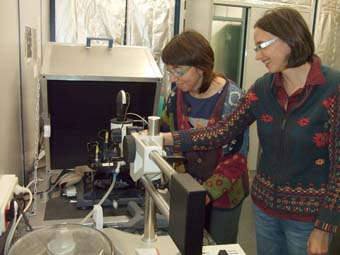
The semiconductor nanowires are structures with a diameter of tens of nanometres and with a length of several microns, similar to a hair but a thousand times smaller. Until now, in order to determine the orientation of these materials it was necessary a complex procedure where the nanowires were one by one analysed. The new technique, that uses an atomic force microscopy and a Kelvin probe, detects tiny forces and measures the electric characteristics of the sample surface. In this way, it is possible to analyse simultaneously the orientation of a large number of nanowires.
As a simile, explains Ana Cros, “this microscopy explores surfaces as a blind person does in order to explores his or her surroundings: it uses a point as a stick, and analyses how it interacts with the surfaces through changes in its vibration. The difference between the microscopy and the stick is that its point is extremely sharp. And if it is also applied an electric potential, it is possible to measure the electrical characteristics of very small objects’ surface without even touching them.
With this technique, known as Kelvin probe force microscopy, was determined for the first time the individual orientation of more than 100 nanowires in the same image.
Núria Garro explaind that “this technique greatly facilitates the analysis and allows to save time: what before took days, selecting nanowires one by one and destroying the sample, now requires only a few hours and the information is obtained without damaging the sample”.
The research is important because the device’s proprieties made with these material depend on their orientation: just like a magnet has two magnetic poles, a polar nanowire presents two electric poles, with different characteristics. Semiconductor nanowires are found between the more studied nanometric structures nowadays. They stand out as basic pieces for the development of optoelectronic devices, from detectors and light emitters to nanosensors.
This work is one of the first results of a new research open line in the ICMUV for the study of optoelectronic processes in advanced materials and surfaces (POEMAS). The study was carried out as a part of the European project NANOWIRING of the PEOPLE programme, leaded in Valencia by Núria Garro.
A. Minj, A. Cros, N. Garro, J. Colchero, T. Auzelle, B. Daudin
Assessment of Polarity in GaN Self-Assembled Nanowires by Electrical Force Microscopy
Nano Letters 15, 6770 (2015); September 18, 2015; DOI: 10.1021/acs.nanolett.5b02607
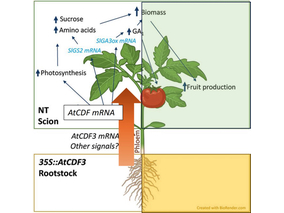
AtCDF3 gene induced greater production of sugars a...
Un estudio con datos de los últimos 35 años, ind...
Un equipo de investigadores de la Universidad Juli...
En nuestro post hablamos sobre este interesante tipo de célula del...
Palobiofarma S.L. is pleased to announce the “last patient last visi...